By Alessandro Vinassa
In a previous article, we saw the importance of galvanic isolation when using an electric field receiver. We also presented a circuit that uses an audio transformer as a solution. And we have seen that the limit of this solution is the low frequencies. In this article we present a technically different solution: an optical isolator: a circuit with a bandwidth of 0,1 Hz – 20 KHz, and its practical application on VLF receivers. Beyond the proposed final solution, the article explains how behind an apparently simple circuit there can be a lot of design effort, to have good final results. The author of the article, Alessandro Vinassa, does not follow the classic style: problem, circuit solution, explanation, but jokingly addresses the difficulties encountered in its design. Are you ready for this original read? Let's go! (R. Romero)
An isolator that starts very low in frequency: 0.1 Hz!
The need of good galvanic isolators is as old as time itself: precisely for this reason Renato and I also clashed with the project of such a device. On August 2023 we started to develop a galvanic isolator apt to receive VLF signals. We have still analysed the simplest isolator possible: the transformer. It is easy, it is silent, but he suffers of distortion and limited bandwidth, especially at low frequency. The main problem we want to overcome is this latter: our goal is to extend the low frequency corner up to 0.1Hz without distortion.
In front of a good beer and a tub of ice cream that our friend Davide provided us (Davide is the engineer who funded us by providing us with great ice cream to eat before, after and during the development sessions), we decided the following specifications for our device:
- Unitary gain, inverting or non-inverting, doesn’t mind, as long as it is known.
- Input impedance higher than 100 kOhm
- output impedance: 50 Ohm
- stable output with capacitive loads up to 10 nF
- input referred noise spectral density lower 500 nV/√Hz
- 0.1% of harmonic distortion
- Max input voltage 316 mVrms (-10 dBV, or 0.894 Vpp, like in a soundcard)
- -3db Bandwidth 0.1 Hz - 20 KHz
Moreover, we decided to supply the device at 24V and to provide an isolated power supply output for the amplifiers on the fields. Truth be told, initially we decided to supply everything at 12V. However, after some thoughts, we decided to switch to 24V to use the isolated DCDC converter we had on the shelves. So, we can add the following constrains:
Input power voltage 24 V
Isolated output power 24 V – 50 mA (1.2 W)
Protection against short circuits, reverse connection, or wrong inverted polarity.
I would have soon discovered that the project was not very fortunate; on the contrary, it has been quite challenging. This is because, to be honest, I underestimated it, forgetting that sometimes circuits with just a handful of components can prove to be much trickier than massive circuits with bus and processors. However, I do not wish to cover my foolishness and am proud to recount the story of this circuit in all its phases.
The article is perhaps a little long, but it should be interpreted as a detective story, rather than as a scientific publication. I think it will be fun. Enjoy the reading!
Chapter 1: first Schematic
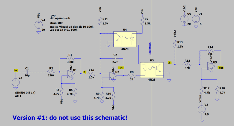
Figure 3: Isolator Schematic. First
Attempt
In Figure 3, I present the first version of the isolator. It is still fraught with issues, and we will work on it, making various changes together. Hence, this is not the final version, which will be unveiled at the end of the article. We'll get there gradually, banging our heads to tackle the problems together, just as I did.
The topology shown above is not new. I saw something similar on an application note of the Avago Technologies (https://docs.broadcom.com/doc/HCNR201-200-AN, link valid on 24/11/2023). The idea is quite simple. We will use two “identical” optocouplers: one to transmit the isolated signal, the other to feedback it. U2 is the driver of the optocouplers’ LED. Since the two LEDs are connected in series, both are driven by the same current.
In theory, considering two identical optocouplers whose LEDs are driven by the same current, they should draw the same current from the output BJTs. So, the distortion present at the output of U4 should theoretically be identical to those at the output of U3. By closing the feedback loop of U2 to the output of U4, the feedback cancels out the nonlinearities of U4. In doing so, it will also correct the nonlinearities of U3, eliminating distortion associated with the components’ non linearityes. I have always said “in theory” since all this reasoning works if the optocouplers are matched, identical.
On the market there is a series of optocouplers called HCNR201 which contains in the same package one LED and two matched photodiodes. But considering that we want to use standard components, we decided to employ the 4NXX optocouplers series, which is normally used as feedback in switching regulators. We will analyse the problem of matching in the next chapter, but for now let’s return to our schematic.
The signal is coupled from C1 to the first stage. This stage is a level translator that shifts the input signal to a 10V offset, that correspond to half the supply voltage. The input impedance of this stage is determined by R2 = 330 kΩ, therefore the low frequency -3dB corner is flow= 1/(2π∙R2∙C1)=1/(2π∙330kΩ∙10μF)=0,045 Hz, which aligns with the specifications. For C2 I decided to use a good X7R ceramic capacitor. U2 is the core of the circuit, and it transfers the signal on node 1 (refer to Figure 3, output of U1) to the node 3 (collector of the isolator U3). This stage can be traced back to an inverting amplifier, with signal’s gain V3/V1 determined by R11/R16 , if the two couplers are identical.
Otherwise, it may undergo small variations related to mismatches, as we will see later. During this simulation I have noticed that to get unitary gain R16 must be set little lower than R11. This behaviour is in contradiction with the previous formula. I didn't care about it, and I simply opted to provide a trimmer in place of R16. Had I known better, I shouldn't have taken this detail lightly. As usual, everything left unexplored comes back to haunt us; we will see this later.
Back to the circuits, U5 finally shift back the signal from 10V (Vbb⁄2) to 0 subtracting Vzero. To avoid complex low frequency response, I decided to AC couple the output stage, leaving only one low frequency pole to limit the bandwidth. A note for the more attentive among you: the operational amplifiers do not have balanced + and - inputs for offset cancellation. In practice, we will use an operational amplifier with very low bias currents, and therefore, this effect is negligible compared to the mismatch among the optocouplers. I've used the same resistances throughout to avoid codes proliferation in the bill of materials.
Chapter 2: Noise simulation
Once the simulation worked, I decided to perform a noise simulation. LTSpice reproduces the noise behaviour of several optocouplers. I choose the 4N28 because I hadn’t a model of the 4N35. I have conducted tests with other optocouplers’ series 4NXX available in spice and I can assure you that the results are all comparable, within the same order of magnitude. Since it is better to settle for something rather than nothing, let's proceed. In Figure 4 we can see the noise plot and the gain plot. The gain is not expressed in dB, it’s a pure number, V⁄V.
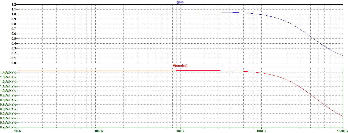
Figure 4: simulation of gain and output
noise spectral density of the isolator.
In this simulation the only “real” components are the couplers and the resistors. Op-amps are ideal: all this noise come from the optocouplers. It’s a huge noise: 1,45µV/√Hz !
After some research, I discover that is well known that optocoupler are not silent components. They introduce various sources of noise:
- Photocurrent Noise: Generated due to the statistical nature of the photons’ arrival at the photodetector. It can cause fluctuations in the output signal.
- Dark Current Noise: Occurs in the absence of light, leading to random variations in the output signal.
- Thermal noise: Arises from the thermal motion of charge carriers in the optocoupler's components, contributing to random variations in the output signal.
Silencing the optocoupler is, therefore, a lost battle. At this point, I wasn't sure how to proceed, but Renato enlightened me, much like what happened to Paul of Tarsus on the road to Damascus. His idea was simple and effective: sacrifice input headroom to decrease the noise. We observed that the noise injected by the optocouplers is constant and not affected by the gain setting. So, we firstly applied a 20dB attenuator at the output of the coupler. The noise decreased by 20dB. But along with the noise, the signal has also decreased! To compensate this unwanted effect, we decreased R16 by ten times, increasing the signal gain of 20dB to restore the unitary gain. In Figure 5 you can see the second revision of the schematic. The output attenuator is made by R14 and R12 on U5
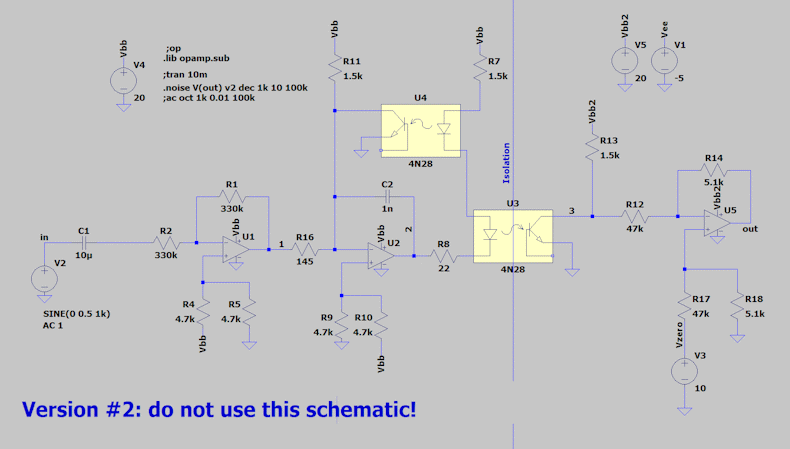
Figure 5: second revision of the
schematic to enhance the noise performance.
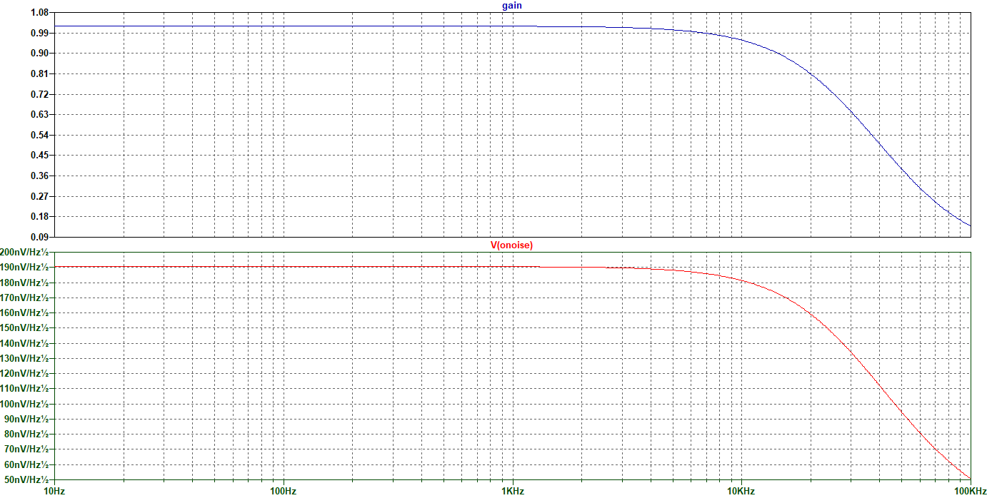
Figure 6: simulation of gain and noise of the second revision
Figure 6: simulation of gain and noise of the second revision
In Figure 6 you can see the noise plot, that is divided by almost the attenuation ratio set by R14 and R12. Now, what are the drawbacks of this solution? We have lost tons of input headroom. In fact, to obtain an output voltage of 1Vpp, we need 9,2Vpp at node 3. A 2Vpp signal would bring the transistor in U3 close to saturation, clipping the output. Therefore, the input signal must be limited at 1,5Vpp to avoid clipping. Moreover, the circuit's power supply, which now is 20V, cannot be lowered too much. It's not convenient to operate the transistor in U3 very close to saturation and cutoff; it's preferable to keep it in linearity.
A 20V power supply is excellent, but it requires feeding the device at 24V to stabilize the 20V Vbb. Ad absurdum, with a power supply of 12V, an internal Vbb of 10V is feasible. The node 3, in this condition, could not have a swing of 9.2Vpp: the optocoupler has not a rail-to-rail output stage, it is an open collector, which can reach the supply rail only in saturation or off-region. At this point, I felt satisfied and decided to consider the circuit valid, although, unbeknownst to me, it presented numerous other errors that I hadn't identified and that we will discover later. However, I decided to tackle another issue: the matching of the optocouplers.
Chapter 3: Optocouplers Matching
Before proceeding, I decided to verify the fundamental assumption of this design: whether two optocouplers taken from the same lot can be considered similar to each other, or more precisely, “almost equal”. I have connected three 4N35 coming from the same reel and having the same date code to my curve tracer, Tektronix 7CT1N and these are the results:
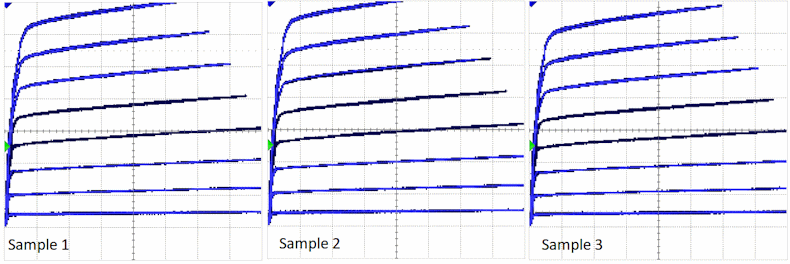
Figure 7: Curve tracer output for three different optocouplers. Y axis: collector-to-emitter Voltage, 2V/div, X axis: Collector current, 2mA/div, 1mA Steps in LED’s current (The lower trace is 1mA, the upper is 8mA)
Despite obvious differences, the curves do not look totally different. We can observe some differences in the upper trace: in sample 2 it tops at 14mA with a Vce of 8V and a Led current of 8mA, while the third one, on the right, reaches only 13.2mA in the same condition (100 (14mA-13.2mA)/14mA=5.7% of error). The positive aspect is that this error seems to be a gain error, and so it is distributed in all the LED’s current steps with the same ratio. Let’s consider the third plot (ILED = 3mA): in sample 2, it reaches 4mA with a Vce of 8V while in sample 3 3,76mA. The percentual error is therefore 100 (4mA-3,76mA)/4mA=6%. I know, this is not a quantitative analysis, but it is quite promising. We can say that the optocouplers are not identical to each other, but their non-linearity can be considered repeatable, except for a gain constant.
“Thus, that's why before, in the simulation, to achieve unity gain, I had to modify R16 from the calculated value! Because the optocouplers can have different gains!” I said to myself, pleased to have grasped the phenomenon. In reality, I was convincing myself of something that could cost me the revocation of my degree! Simulations are the only places where all components are ideal, and therefore, the cause of the strange value of R16 cannot be related to components matching. At this point, it's better to gloss over, blame it on the heat of August, and proceed to the next chapter, where we will see the PCB that houses the circuit, with its problems still partially unknown and partially mysterious.
Chapter 4: The PCB, first test.
The PCB is composed of two parts: the power supply and the isolator. As you can see, it is not much different from the one we simulated. On the secondary side, I have an unused op-amp, so I decided to buffer the zero trimmer R20. This is entirely useless; I should have thought more carefully about what to do with that half op-amp.
The input and output connectors are BNC for signals and DC-Jack for the power supply.
I decided to try to filter the input and output power using common mode filters. Two Schottky diodes protect the board against reverse power connection, while two fuses limit the short circuit current.
For clarity, let's reiterate the directions of the various signals. The power supply originates from J2 on the 'lab side' and is brought to the 'sensor side' through the isolated DCDC converter IC4. Here, it is used to generate the 20V supply via an LM317 and to power other devices in the field through J1. Conversely, the signal enters via the BNC X1 from the 'sensor side' and is output to X2 on the 'lab side.' On the lab side is generated, in addition to the 20V supply, also a -5V to give a negative supply to the output stage which is DC coupled.
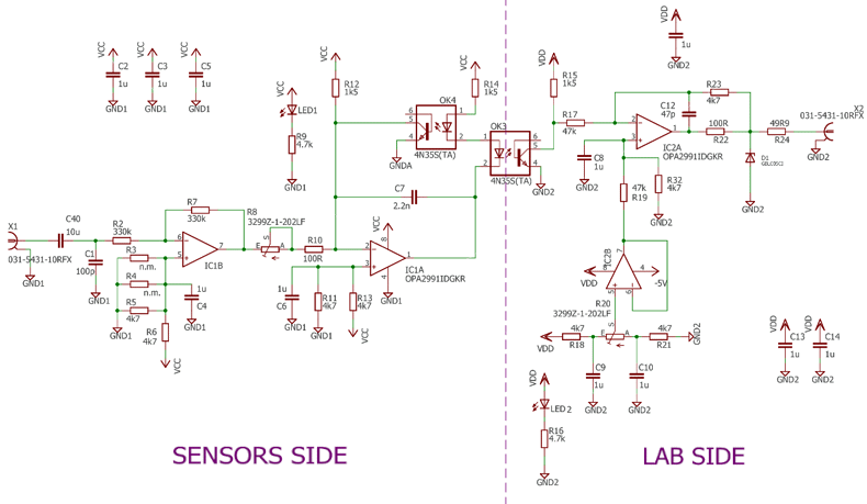
Figure 8: PCB schematic, signal path
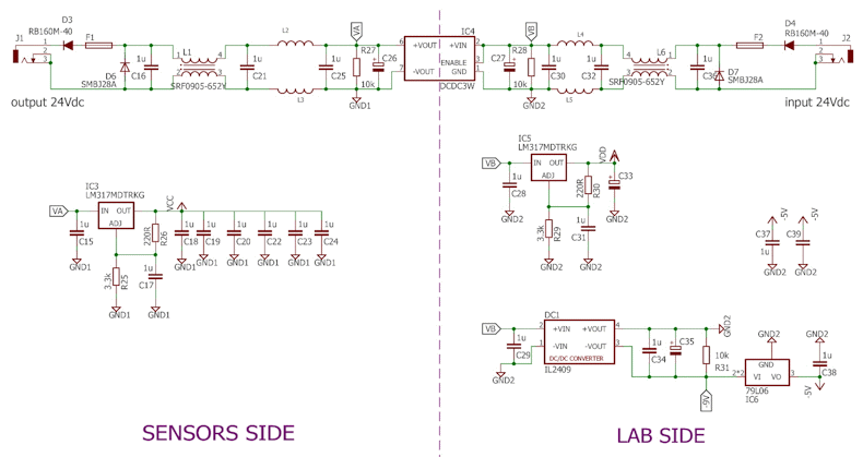
Figure 9: PCB schematic, power supply.
I don't think it's necessary to dwell further on the schematic. In particular, we won't discuss how to design a common mode filter of this kind. If anyone is interested, we could address it in another article.
Fact is, I decide to have 5 prototypes manufactured and assembled by JLCPCB. As soon as they arrive, I notice a first distraction error. I did not connect two traces on the optoisolator OK3. JLC, in fact, did not have the 4N35 through-hole version available, so I replaced both couplers with SMD ones. In my haste, two traces left in my mouse. Not a big issue. It's the usual problem of doing things in bits of spare time. A quick jumper wire and we're back on track.
After the last components not provided from the low cost supplier were assembled, I connected the power supply and a test signal. It worked! With the help of the oscilloscope, I regulated the gain and zero trimmers without any problems. Then I measured the low frequency corner: 290mHz. It was off by 5 times compared to the design value. I checked the schematic, I checked the BOM assembled by the low cost supplier, I checked the simulation. Everything was correct. The value should be around 0,05Hz, but it was at 0,29Hz.
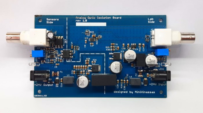
Figure 10: Final assembly, according to the
two schemes. The upper part is related to the signal,
the lower part to the power supply. The dotted line
indicates the separation between the two sides: sensor
and laboratory.
Chapter 5: The Mystery of the wrong pole
With the scope I observed that the anomaly was generated between the input capacitor C40 and R2 (referring to Figure 8). Is this filter wrong? Because, at that point, the rest of the circuit does not seem to change the amplitude. So, I measure R2 and it turns out to be 325kΩ. Perfect. Thinking that the issue could be with the capacitor supplied by low cost suppliers, I decided to replace it with one I already have from a trusty brand: 10µF ±15% X5R, 25V 0603, produced by Murata (GMR188R61E106KA73D.). I re-measure the pole: 0.26Hz. I set the heavy artillery and measured with my trusty HP8751A the Murata capacitor that I had just soldered in place of the cheap one. In Figure 11 you can see the impedance plot of the Murata capacitor, in modulus and phase. At 100Hz it shows a totally complex (- 90° of phase) impedance of 156Ω. Hence the capacitance can be calculated as 1/(2π∙156Ω∙100Hz)=10,15µF. Thus, the capacitor value is correct, everything is correct, but nothing works.
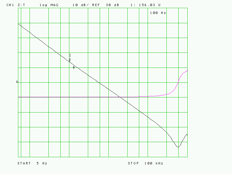
Figure 11: Single capacitor measure with
network HP8751. It shows a complex impedance of 156Ω @
100Hz
The night brings counsel, and the next day I wake up with an intuition. Ceramic capacitors may exhibit piezoelectric behaviour, which means they can undergo mechanical deformation in response to an applied DC voltage. In ceramic materials, the crystal lattice can experience a physical distortion when subjected to an electric field, leading to a change in capacitance. In short, the application of a DC voltage modulates the capacitance of the ceramic capacitor.
In our circuit the capacitor is stressed by a 10V DC potential, as explained in Figure 11. The noninverting input of IC1B is fixed at 10V from a voltage divider. Since the non-inverting pin follows the inverting pin, the inverting pin of the operational amplifier is also at 10V. And since there is no current flow in R2 (for DC, of course), there are also 10V on one side of capacitor C40. On the input side, however, we are connected to the signal generator, which is at 0V relative to ground.
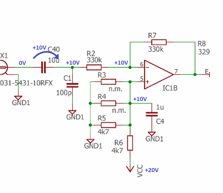
Figure 12: DC stress of input capacitor
Can this polarization change the behaviour of the high-pass filter? To prove this theory, I build the simple circuit in Figure 13.
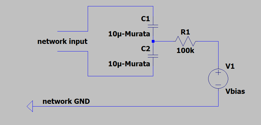
Figure 13:Test circuit for capacitor
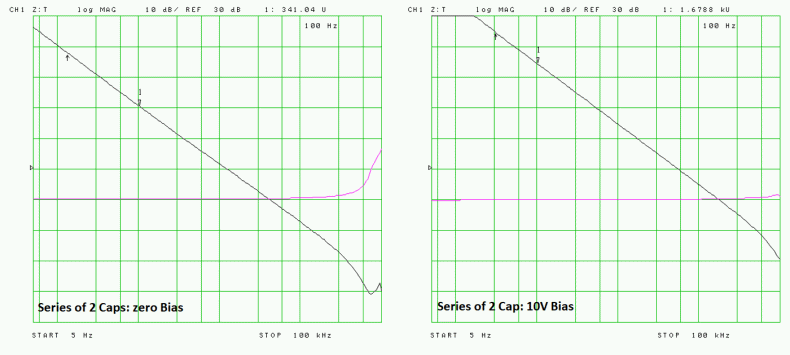
Figure 14: measure on test circuit. Two
X5R capacitor with and without bias.
In this set up, a series of two identical capacitors is connected to the input of my network analyser. On the central node I can inject the bias voltage with a DC power supply while the 100k resistor ensures that the power supply does not affect the measurement of the capacitors. Without bias we can read an impedance of 341Ω at 100Hz corresponding to a total capacitance of 4,667µF. But with 10V the impedance strongly increases up to 1678kΩ at 100HZ: 0,95µF for a series of two capacitors. This means that one capacitor biased at 10V has a capacitance C_bias=1,9μF and the -3dB low frequency pole in our circuit is:
flow= 1/(2π∙R2∙Cbias) =
1/(2π∙330kΩ∙1,8μF) = 0,253Hz.
Mystery solved. To be honest, I knew this phenomenon exists, but I didn't think it could have such a significant impact. We measured an 82% reduction. What to do? I can either install an electrolytic capacitor or mount multiple capacitors in parallel. I decided to replace it with an electrolytic capacitor. I had a bag of 33μF 63V low ESR capacitor on hand. I installed it with the positive pole facing towards the 10V, considering that the input signal should be free of bias, and I added a 1MΩ resistor between the input and ground to avoid an excessive charge of the capacitor if left floating.
Chapter 6: The mystery of wrong gain and high distortion
In the meantime, we've also sorted out the bandwidth. Now I decide to test the distortion of our isolator. I tested the device with 100mVrms and with 320mVrms, which we decided to be the maximum. The results are given in the following plot:
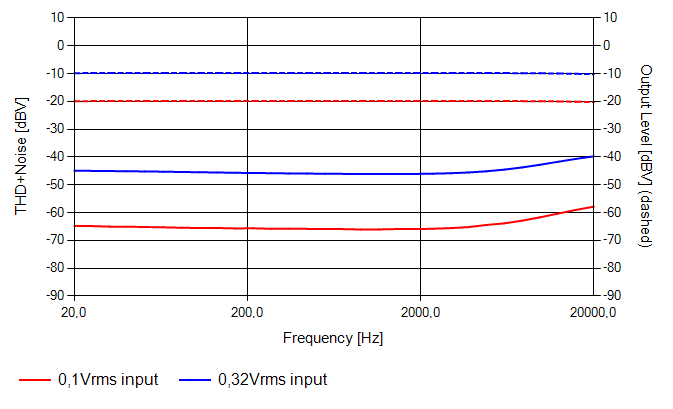
Figure 15: distortion of the isolator
It was not a complete disaster, but THD is near -45dB, that means 0,56%. Looking at the graph of Figure 15, at higher frequency, where the op-amp’s loop gain starts to decrease, it reaches 1%. Let it be clear, a distortion of 1% is indeed very low, not visible to the naked eye on an oscilloscope. Many vintage audio amplifiers have higher distortions, and many vintage oscilloscopes have vertical amplifiers with higher distortions too! However, it's always worthwhile to try and understand things as much as possible. Back to the plot, I understand that distortion may increase at high frequencies, and I can accept it, considering that these harmonics above 20kHz will likely be filtered out by the anti-aliasing filter of the audio interface.
However, at low frequencies, it would be nice to reduce THD. The question is: what, at low frequencies, where the operational amplifiers have tons of loop gain, could generate distortion? The obvious answer: apparently, the optocouplers are not as identical as I thought. I de-soldered the two isolators and replaced them with a pair I selected using the curve tracer. I thought this would reduce the distortion. However, no, nothing appreciable, still 0,5%. Yet the optocouplers now were matched: at the same Vce and drive current, they draw the same current from the output collector. The drive current is identical in the circuit, due to series driving. But what about Vce of the output BJT? Perhaps I had found the error. Let's look at the schematic, in Figure 16
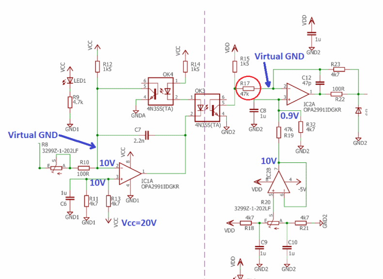
Figure 16: Analysis of the schematic to
understand the mystery of wrong gain and high distortion
Let's examine the circuitry around IC1A: the non-inverting input is fixed at 10V. The feedback keeps the inverting pin fixed at 10V too, making it a virtual ground. The input signal is injected in the form of current through R10 into the virtual ground. To keep the inverting input at a constant voltage, the feedback modulates the current of optocoupler OK4 absorbing any excess of current or supplying the missing one via R12. But the key point to observe is that the voltage on the collector of OK4 is always consistently held at 10V, regardless of the input signal. Its load line is a vertical straight line, meaning that, whatever the LED current is, Vce can’t be different from 10V. You can see it drawn as a red line in Figure 17.
Moreover, on the secondary side, the inverting input of IC2A is a virtual ground, kept constant at 0.9V by the feedback. But, between the OK3 collector and the virtual ground there is a 47kΩ resistor, R17. This means that the load line of this isolator is a resistor which value is the parallel of R17 and R15: 1453Ω (Figure 17 in green). Even two identical devices cannot behave in the same way if loaded differently. And this is also why the value of the gain resistors didn't match even in simulation: two different load lines definitely lead to different gains. So, if we could make these two load lines equal, we should further reduce distortion and also regularize the gains. Too bad I didn't think of it earlier.
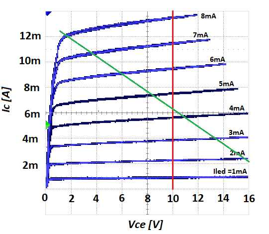
Figure 17: Load line of optocoupler OK4
(primary side) in red, load line of optocoupler OK3
(secondary) in green.
Since we already have the printed circuit boards in hand, we need to come up with a quick and functional modification. Making the load line of the secondary side vertical is impossible, so it's better to bend that of the primary. Secondly, we can also limit the bandwidth of the output stage to 22kHz -3dB, to slightly reduce the harmonics’ content above 11kHz. Limiting the bandwidth in a signal that will be sampled is never a sin.
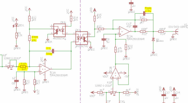
Figure 18: final arrangement of the
schematic
The result is shown in Figure 18. I added R999 to get the same load line for both the couplers. Well, in this way the load lines are parallel, but not coincident, because R17 is connected to a virtual ground of 0.9V, while R999 to a virtual ground of 10V. This produces a shift between the two lines of 200μA, which is completely insignificant with respect to their bias current of 6,66mA. In any case, the situation is infinitely better than before, when the two load lines formed a Saint Andrew's Cross!
I also change the value of R10 (which in always in series with a 2kΩ trimmer) to minimize the noise. Now the gain of IC1A is -R999/R10 = -47kΩ/4,7kΩ= -10, while the IC2A has a gain of -R17/R23 = -4,7kΩ/47kΩ= -0,1. Considering that the first stage has gain -1, the total gain of the system is -1: inverting unitary gain. And this is true even in simulation without trimming resistors. The mystery of gain has been solved. But what about the distortion? We can see the response of the distortion analysis in Figure 19.
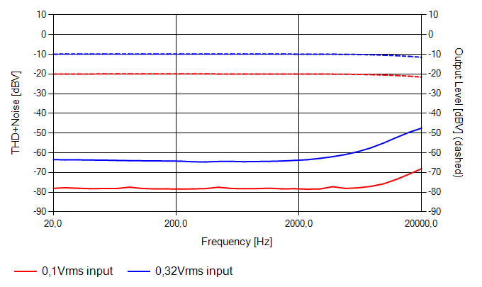
Figure 19: Distortion of the final arrangement of the isolator
With an input of
0,1Vrms, the distortion is beyond -75dB, which is
0,017%, and then it reaches -65dB (0,056%) at high
frequencies. Applying the maximum signal, 0,32Vrms,
the distortion is less than -60dB (0,1%), reaching
0,5% at 20kHz. The measurements are taken considering
all harmonics up to 80kHz. A satisfactory result that
makes the device usable even for audio.
Chapter 7: Last measurements
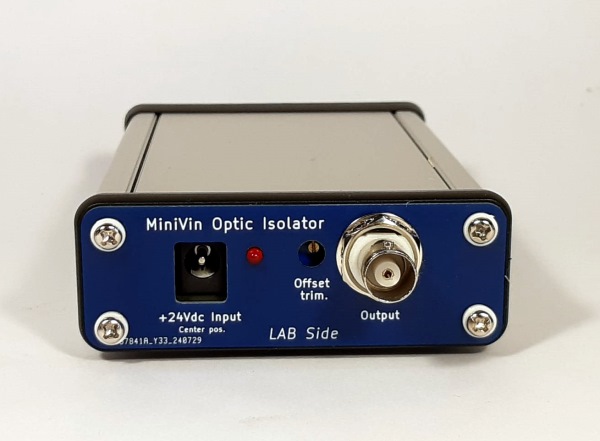
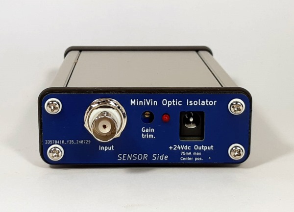
Figure 19bec: Final assembly: lab side and sensor side
We are approaching the end of the project, and we have solved all the problems that have arisen. Some other checks still need to be done: bandwidth, distortion at very low frequencies, saturation voltage, and finally noise. I will spare you all the measurements of the power supply section. They are rather tedious. However, we will perform the noise measurement at full load. Remember that the board, in addition to isolating the signal from the field to the laboratory, also provides an isolated power supply to the field: 24V 50mA.
Let’s start with bandwidth. The high frequency limit is 28kHz, perhaps even too much.
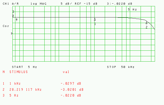
Figure 20: High frequency response of the isolator
The low frequency corner is near 15mHz (actually, we use a 33µF capacitor with a 330kΩ resistor, whose pole is 14,6mHz). This is remarkable, but it causes rather long transients (some tents of seconds, because of the time constant of the filter R∙C=10,9s) when connecting the isolator, forcing us to wait for the capacitors to charge/discharge at the right value. However, this bandwidth can be easily reduced by changing the capacitor itself. In Figure 21 is shown the VLF behaviour at 15mHz: it seems we are looking at a voltage follower. Distortion seems to be absent.
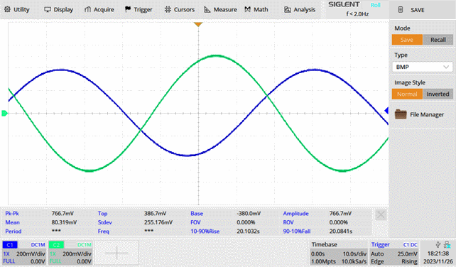
Figure 21: 15mHz sinewave. The green one is the input at 1Vpp, the blue is the output at 0.7V, near the -3bB limit.
Note that the Timebase is at 10s per division!
For what concern the maximum voltage before clipping, it seems that the device enters compression before hard-clipping. In any case, at 530mVrms input signal, it is still in linearity. At 570mV, it begins to compress the upper half-wave. The Figure 22 shows the isolator output at 0,6Vrms: the compression of the output (blue) begins to be visible. Considering that we had set out to transport signals of 320mVrms, and the object still supports signals up to 570mVrms, we can consider ourselves satisfied.
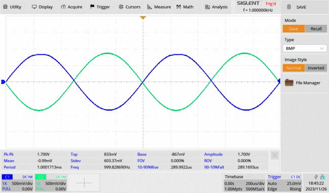
Figure 22: Compression of the output at 1kHz. Green: input 600mVrms, Blue: output
The last thing we have to measure is the noise. I have made two plots: the first represent the high frequency noise, for frequencies higher than 1kHz, the second represents the low frequency noise for frequency lower than 300Hz. The noise in shown as voltage noise spectral density in μV/√Hz. During the measurements the isolator has a 50Ω termination mounted on its input. The first plot (Figure 23) displays a noise of 0,35μV/√Hz, which is better than what we expected.
At low frequencies, something different occurs: it is observed that the noise below 200Hz starts to rise with a slope of 10dB per decade. Therefore, the corner frequency of the device is 200Hz, and beyond it, the flicker noise component prevails. This increase in noise can also be explained by considering that our device is DC-coupled, except for the input capacitor, which now we ignore.
Mathematically, it can be demonstrated that flicker noise is correlated with the phenomenon of "random walk”. This means that the output of the device is not constant but fluctuates due to a random process, by a few microvolts. In our case, frankly, I haven't investigated where the phenomenon comes from: certainly, operational amplifiers contribute their part. Even optoisolators are probably affected by this type of noise. However, the noise is still very low compared to that of the audio cards commonly used for sampling in VLF.
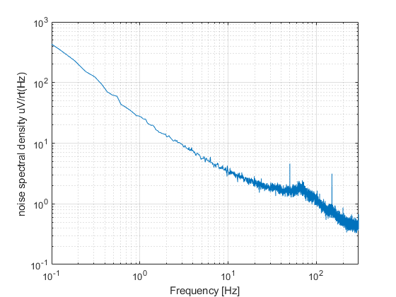
Figure 23: Low frequency noise spectral
density of the isolator.
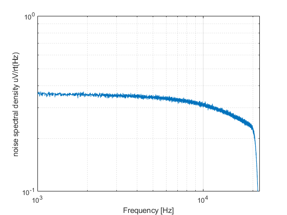
Figure 24: High frequency noise spectral density of the isolator.
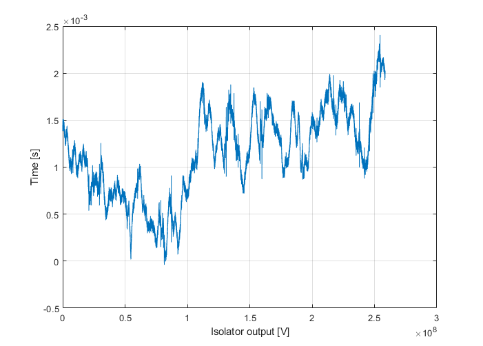
Figure 25: The random walk shown from the isolator
To better understand the phenomenon, I plotted the output voltage from the isolator in the time domain (Figure 25). Looking at the image, the origin of the term "random walk" is clear! Compared to the noise declared by Texas Instruments for the AMC1311, we have to accept a defeat. The Texas circuit does not show flicker noise; it uses a topology based on sigma-delta conversion, which is capable of “cancelling” flicker noise. Nevertheless, the device is certainly usable, and therefore, we can consider ourselves satisfied!
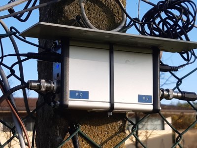
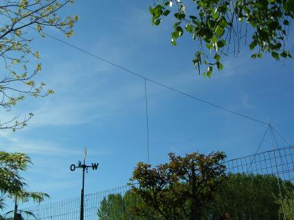
Figures 26 and 27: The isolator positioned outside, at the base of a 10-meter high Marconi antenna with a 15-meter top hat and a LNVA_20-24 receiver (http://www.vlf.it/cumiana/romero_LNVA.pdf).
Chapter 8: Conclusions
Now the question is: how many of you figured out the cause of the mysterious malfunctions before it was revealed? Jokes aside, first of all, thank you for joining us on this journey—a bit long, a bit winding, but definitely very human. We've created a useful device for our setups, and at the same time, we've delved into some uncommon aspects of modern electronics: load lines, capacitor non-linearities and more. I hope this unconventional approach was appreciated.
There are several possible modifications to the device: connecting both optoisolators to a virtual ground to allow for powering the circuit at 12V, or trying to eliminate flicker noise, perhaps using a chopping system. Another option is to implement a sigma-delta modulator to digitize, transfer, and reconstruct the signal.
In any case, regardless of the results, we hope to have been thought-provoking and helped you spend some peaceful time reading something a bit different! Of course, if you enjoyed the article and would like to see this isolator evolve or be simplified, if you’d like further explanations, or if you have ideas, feel free to contact us: we'd be happy to bring you new articles on topics of interest!
Return to www.vlf.it main index