The best compromise between sensitivity and portability
by Luca Feletti and Renato Romero. PCB layout by Jochen Richert, Phil Gillaspy, Valerio Cammelli and Maurizio Pallotta.
 |
|
This project is the EASYLOOP receiver
evolution, made in 2002 and built again and
again by many VLF listeners: despite its
simplicity, it has given great satisfaction,
receiving whistlers, chorus and others natural
radio signals. If you think it's time to have
something more read this article: the IDEALLOOP
H301 is a compact loop to receive VLF. It is
small and portable but with great performances:
up to 15 dB more sensitive than Easyloop and an
incredible 8 Hz to 20 kHz bandwidth flatness,
with only 50 x 50 cm space. It's able to receive with great sensitivity all classic natural origine radio signals: whistler, chorus, tweeks, and even in the background Schumann resonances. In addition of course to all the man-made signals such as military, RTTY radio navigation signals and SID effect on it. |
We started with some considerations: a wide-band loop antenna with good performances is given by a proper loop/preamplifier matching, and an adequate turns/size dimensioning to overcome the loop intrinsic thermal noise and the operational amplifier input noise. Size, copper weight, number of turns and wire section are the loop elements that determine the final result. But it is not all: loop receiver and preamplifier circuit are to be considered all in one: the preamplifier is not a generic preamplifier, it is THE preamp for that loop. There are many parameters contributing to a proper functioning of the system, and they are closely connected one with another.
For example: by increasing number of turns we increase the capturing area then we get more signal, but at the same time we decrease the self resonating frequency and we increase as well the system impedance. If the impedance grows, noise increases too induced by operational amplifier current noise. In few words, by maintaining the same operational amplifier: sometimes more turns can cause less sensitivity. It does seem impossible but it's true!
The loop impedance is in fact another very important parameter. In addition to thermal noise generated by the resistance of copper wire, we must also deal with the noise input of operational amplifiers: it is strongly influenced by the source impedance, and the value of S/N can vary by tens of dB the impedance. The impedance should be a manageable values for the whole frequency range in which we want to run our loop.
2) LOOP DIMENSIONS AND ELECTRICAL VALUES
Our project is based on a natural background level of expected signals at 1 kHz of -30 dBpT (0.03 pT, Maxwell and Stone 1963, http://www.vlf.it/naturalnoisefloor/naturalnoisefloor.htm): we want obtain the best compromise between size and sensitivity. The sensitivity formula to determinate the number of turns, by the voltage at the terminals of a loop immersed in a known field, is always the same:
N is the numbers of turns in the loop
A is the area of the loop
in square meters
f is the frequency in Hz
H is the magnetic field
in A/m ( B[µT] x 0,796)
After all said and done we decided that a good
portability and a good sensitivity are achieved with 1/2
kg of copper on an area of 0.25 square meters. Have to
be considered valid in this regard the remarks made in
the design of Minimal Loop (http://www.vlf.it/minimal/minimal.htm): loop sensitivity is determined by the weight of the copper
used for occupied area.
A single turn square loop, 1m side, made with 1kg copper
has the
same sensitivity of a 1000
turns square loop made with 1kg copper and same
dimensions. In this context,
the sensitivity limit
is represented
only by loop thermal
noise:
If we had an
ideal preamplifier
(free input noise) the
reasoning would be over here, but
it is not yet: loop
impedance (and therefore the turn number) influences
the noise of preamplifier input, then the
noise figure, and then the
final sensitivity of the device itself.
Size and weight of copper loop must be decided according
to wire diameter available, which is more
appropriate: many turns of fine wire or few turns of a
thicker wire. Few turns mean lower voltage received, low
impedance, but low resistance, than low thermal noise
and high self resonance frequency. Many turns mean: more
voltage across the loop, but higher resistance (then
higher thermal noise), higher impedance, lower self
resonance. Our choice was determinate therefore by
system impedance: loop signal will be amplified
and all the best amplifier devices operate with low
noise performance with impedances of medium value.
Our choice has therefore focused on these final
dimensions and characteristics of the loop we are going
to build:
- Shape: squared (for mechanical reasons: the
support it is easy to build)
- Side: 47.5 cm (big enough for good area
capturing, but sufficiently small to be portable and
easy to carry)
- Turns number: 235 (enough for give good
sensitivity and not prohibitive impedance, but less
enough to keep self resonance above 20 kHz)
- Wire: enameled copper wire 0.4 mm diameter (AWG
26), 446 meters, 0.5 kg (low resistance of 60 ohm, which
implies low thermal noise and thus high sensitivity)
There are many formulas to calculate the value of wire
resistance and inductance. Design and dimensioning of
the circuit was based on these values; see for example
computer programs written by G4FGQ (http://www.zerobeat.net/G4FGQ/):
- Inductance: 80 mH
- Resistance: 60 ohm
- Loop Low Frequency corner : 119 Hz (frequency
where the inductive reactance and resistance reach the
same value)
- Parasite Capacitance: 435 pF (deducted by
estimated loop self resonance frequency)
- Thermal noise: 0.98 nV in 1 Hz RBW
- Sensitivity @ 1 kHz with an ideal preamplifier
(no noise): 0.0029 pT in 1 Hz RBW
- Sensitivity @ 10 Hz with an ideal preamplifier
(no noise): 0.29 pT in 1 Hz RBW
At the end the measurement on
the loop with a HP 4274A bridge, built as above, confirmed
these values:
| Freq [Hz] | L [mH] |
Q | Z (module) [ohm] | L [mH]
(2nd Loop) |
| 100 |
80.94 |
0.8 |
79.8 |
79.50 |
| 400 |
80.08 |
3.1 |
211 |
78.8 |
| 1000 |
80.9 |
7.1 |
503 |
79.7 |
| 4000 |
79.7 |
16 |
2000 |
79.4 |
| 10000 |
85.0 |
13.9 |
5320 |
82.0 |
The loop was constructed duplicate, to create a RDF system: one will be placed in NS direction and the other one orthogonal to it, in EW direction. From the comparison of inductance values it is clear that it is virtually impossible to build two identical loops, also using the same turn number and two similar frames. We shall see later that this is not quite a problem.
 |
With the same
instruments, measured capacity between loop
conductor and aluminium tape shielding was 510
pF (here in the circuit splitted in two 255 pF
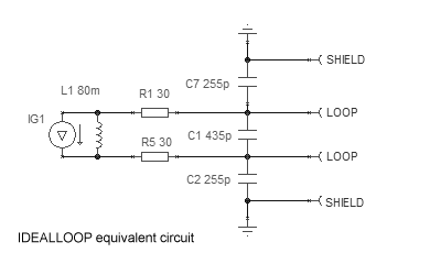
capacitors). We can so imagine the equivalent circuit as shown beside, where R1 and R5 are the copper wire resistance, L1 is the loop inductance, C1 is the parasitic distributed capacitance between the loop turns, and C2 and C7 are the capacitance between loop and shielding. |
Knowing the values of our loop we are now able todetermine the impedance at various frequencies. This data helps us to choose the operational amplifier according to the input noise, voltage and current. There are many ways to calculate the loop impedance at various frequencies. We can use the formulas, since we know the values of the equivalent circuit. Or we can use a simulator to determine this value. A very simple and free software to use is "RFsim99". It analyzes the circuitry in very similar way to a network analyzer, providing the S-parameters and the impedance values. Here is our loop simulated with RFsim99 and the graph of its impedance. Accurate impedance values are obtained by moving the horizontal cursor in the panel to the desired frequency.
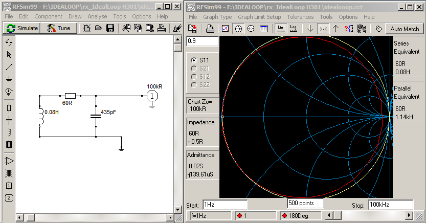
Here in the following table there are impedance values obtained with RFSim99 and the value of Z module obtained from the quadratic sum of the two values.
| Freq [Hz] | R [ohm] |
X [ohm] | Z (module) [ohm] | Behaviour |
| 1 | 60,00 | 0,5 | 60 | Resistive |
| 3,3 | 60,00 | 1,5 | 60 | Resistive |
| 10 | 60,00 | 4,99 | 60 | Resistive |
| 33 | 60,00 | 16,56 | 62 | Resistive |
| 100 | 60,00 | 50,27 | 78 | Resistive/Inductive |
| 330 | 60,02 | 150 | 162 | Inductive |
| 1000 | 60,23 | 509,98 | 514 | Inductive |
| 3300 | 62,55 | 1690 | 1691 | Inductive |
| 10000 | 80,63 | 5830 | 5831 | Inductive |
| 33000 | 243,74 | -33100 |
33101 | Capacitive |
| 100000 | 0,37 | -3950 | 3950 |
Capacitive |
Note: the resistance evaluated by the simulator is the real part of the equivalent bipole impedance and it’s equal to the loop resistance only far enough from the loop resonance frequency. But if instead of using software, you prefer to manually calculate them, here you have the formulas:
Let’s choose the operational amplifier, selecting low-noise models and see how they behave with our loop.
3) NOISE EVALUATION
The choise of the right operational amplifier is a delicate operation: this matter affects the sensitivity of the apparatus we are going to build. Each operational amplifier type has its own specific noise voltage at its input, and the same applies to the current noise. These values change with frequency: for each single frequency the total noise input is given by the square sum of:
- voltage noise from thermal noise loop resistance
- voltage noise generated by opamp
- voltage noise caused by current noise of the opamp, that flows in the loop impedance
These value applied to the voltage/field loop formula (reported above), and loop impedance, will give us the loop sensitivity at each frequency. Here the results with the most commune low noise operational amplifier: OP27, AD743 and AD797.
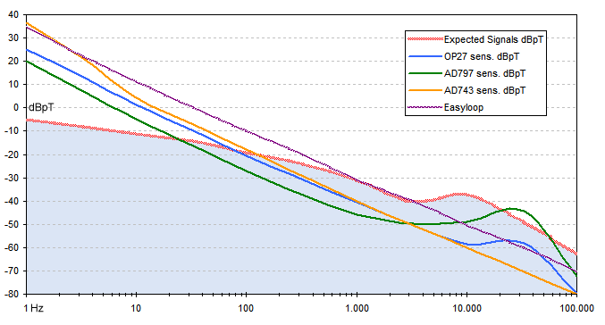
We have also assembled, for the following verification test, a "dummy loop". It was built to simulate the electrical specifications of the loop (inductance, resistance and parasitic capacitance) but screened to magnetic signals. Just like our aerial loop: 80 mH, 60 Ohm and a self resonance frequency of 24 kHz. In practice, a deaf loop, that does not receive. It will be used by us to check the input noise floor of the preamplifier.
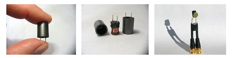
Attention: these small "olla type" coils perform a very high inductance because inside them the magnetic flux has a closed circuit, as in a transformer (the cover is made by ferrite too). For the same reason, they can not be used to receive signals, singly or in array. But this is just what we need. Our dummy loop is made by a single 80 mH inductance (58 Ohm resistance itself) and a 330 pF capacitor in parallel (the green one in the last picture).
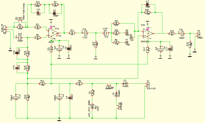
4) PREAMPLIFIER CIRCUIT
Here is the preamplifier circuit.
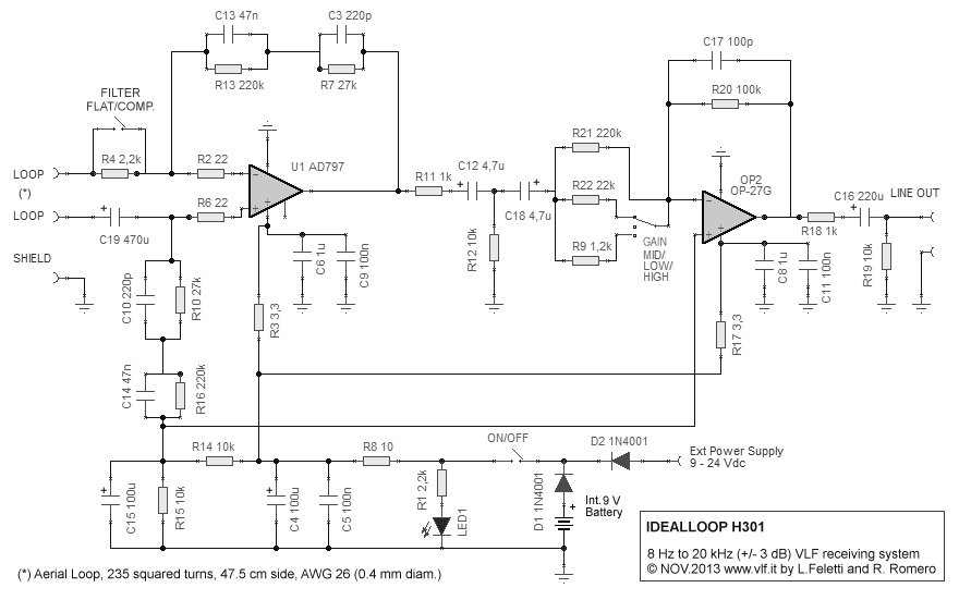
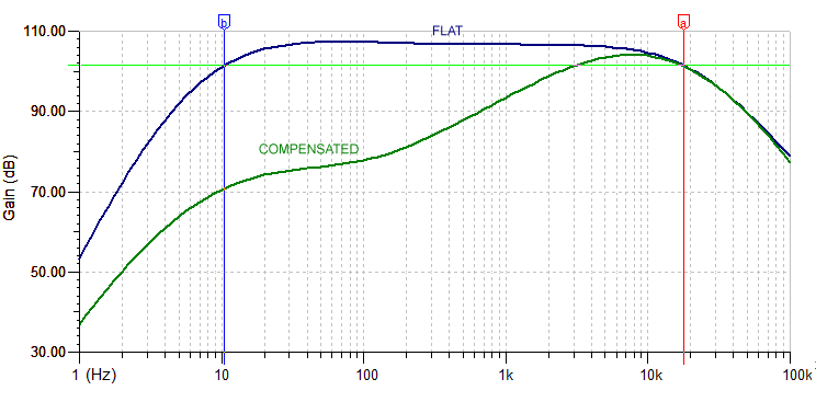
The chosen circuit configuration is what is called "balanced differential". It provides many advantages for our type of loop, first of all creates a high common mode rejection of signals. Magnetic signals effectively picked up from the loop are amplified, while those ones introduced improperly, for example by capacity way, are rejected. In short terms: the antenna is very sensitive to magnetic field, but almost totally deaf to electric field and disturbances coming to it through the power supply (if it is fed directly) or by cable connects to the PC.
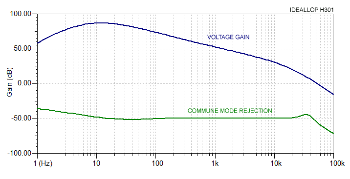
In the graph we see how received signals are amplified (in voltage) by the loop (blue trace) and how those captured in common mode (green trace) are rejected: voltage ratio between received signal and rejected signal, remains greater than 80 dB from 1 Hz to 10 kHz.
There are two available frequency responses: FLAT and COMPENSATED. The insertion of the filter "COMPENSATED" induces a frequency response that compensates gain in function of expected signals level, according to indications of Maxwell/Stone graphs in the famous paper of 1963 (http://www.vlf.it/naturalnoisefloor/naturalnoisefloor.htm). From 1 Hz to 10 kHz the dynamic signals range are usually greater than 30 dB, while with filter inserted, the entire range of the signals is contained in 10 dB.
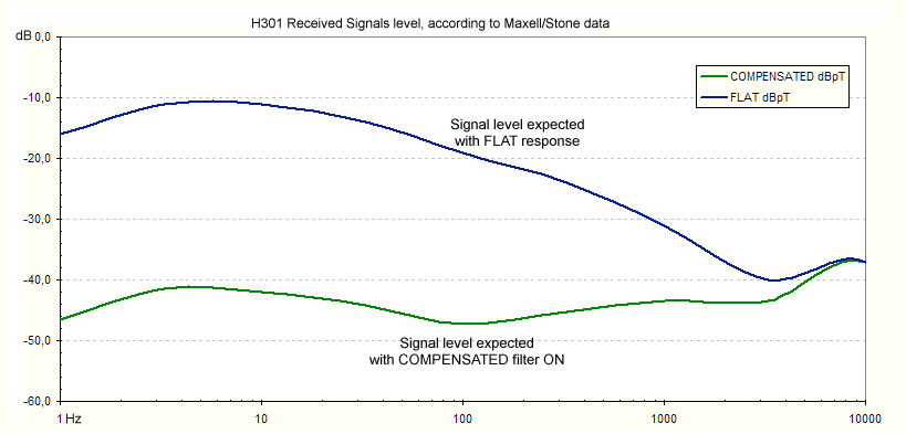
It allows a better utilize the dynamics of the sound card and obtains a spectrogram with a better visual quality. The filter insertion is also useful in case of hum noise: signals at industrial frequency (50/60 Hz) and strongest harmonics are 30 dB attenuated. The compensated filter affects directly the first stage gain: unwanted signals such as hum noise are therefore reduced before being amplified. The result is that with the filter inserted the circuit is not saturated even in presence of high hum noise values, such as the interior of a house. This causes a decrease in sensitivity at low frequencies, but it allows to use the receiver even in severe environments.
Here at last the final frequency response of the entire system, respect to an incident magnetic field:
We have a flatness frequency answer from 10 Hz to 20 kHz in +/- 3 dB. This means we can use this loop also as a measurement loop: knowing the antenna factor we are able to calculate the magnetic filed in pT measuring the signal output level in mV simply with a portable multimeter, but we will see this later on.
 |
|
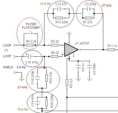
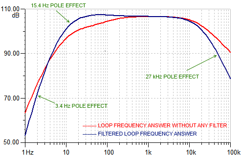
The "secret" of this circuit is all is contained in the input stage: it is modeled as a function of the loop parameters. Let's see how. Reaction network is divided into two symmetrical parts, electrically above and below the loop, allowing it to float. Every part contains a RC cell with a cutoff frequency of 27 kHz and a gain of about 60 dB at low frequencies (red circles), and RC cell with a gain of 77 dB up to 15.4 Hz (green circles). This second part is used to equalize/compensate the cutoff frequency of the natural loop, that, without this network due to its intrinsic resistance, would be of 120 Hz. |
 |
The network extends the
frequency response down to few Hz: it only
operates up to 15 Hz, after which the
capacitor shorts out and it becomes transparent.
The capacitor C19 does not enter into resonance
with the loop: it simply reduces the frequency
response under 4 Hz, avoiding manually moving
loop goes it into saturation, due to the Earth's
magnetic field. Finally R4, placed in series with the loop, worsens the Q system, lowering the sensitivity at low frequencies and obtaining the COMPENSATED curve response. R2 and R6 do not contribute to frequency response: they only act to protect operational inputs, incase of strong current transition, when a local storm occurs. |
Gains have been calculated so that the first stage output noise is likely to prevail over input noise of second stage. This condition provides the best noise figure available. At the time the overall gain was set so that total noise output from the second stage, exceeding the sound input noise. No output signal from one stage must be limited by one noise input to the next: this is a good rule to keep in mind when designing circuits, always.
The second stage allows three gain levels, differentiated from each other by 20 dB. This means that, starting from the mean one, we are able to attenuate the signal by 10 times in voltage, or amplify it, always 10 times. This allows the loop to operate without saturating in almost all environmental situations:
- in a
desert area away from power lines with very high
sensitivity (HIGH)
- in the
backyard of your country home with good performances
(MID)
- and
within serious limits also on a city balcony (LOW)
receiving in prevalence network noise, as obvious.
In this chapter we describe the mechanical construction of the instrument. For convenience, we shall make the description following the path of the signal we are interested and we shall do using the block diagram of Fig. 6.1.
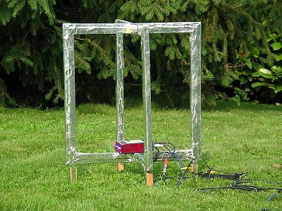
The first part encountered by the signal is the loop system. We have provided a loop for each axis we are interested in.
Since we are interested in possible applications of RDF (radio direction finding) we have made two orthogonal loop; obviously the system works with a single loop also, if our interest is only in one of the three spatial components of the magnetic field.
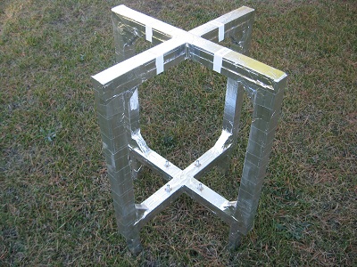
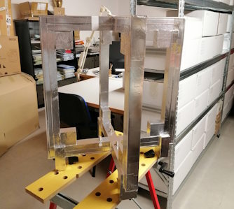
The loop structure is constructed with two square wood support, mounted orthogonally one to the other. Each side of the square is formed by a strip of beech wood having a cross section of 45 mm x 20 mm and a length of 47,5 cm. In the lower side of each square support we have provided two holes for threading the ends of the winding and two little wooden support legs.
All the wood parts are assembled without metallic junction elements, but using only wooden dowels and glue. Over each side a PVC cable duct (provided with a lid), having dimension of 40 mm x 25 mm, is fixed using acrylic adhesive. 235 turns of 0,4 mm diameter (AWG 26) enamelled copper wire are located within the duct with their ends threading trough the said holes. The Fig. 6.2 and 6.3 show what described.
 |
|
| FIG. 6.2 The double loop system for biaxial application | FIG. 6.3 Loop assembly diagram |
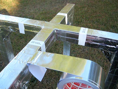
When we have finished the winding, we have mounted the lid on the duct and provided to shield the entire structure of the orthogonal loop with an aluminium adhesive tape. This shield is useful against the effects of the electric field (we want to receive the magnetic field) and we have paid attention to discontinue it in four point to avoid the formation of a close loop in the shield in which a current, due to the variation of magnetic induction, would flow desensitizing the entire receiving system.
 |
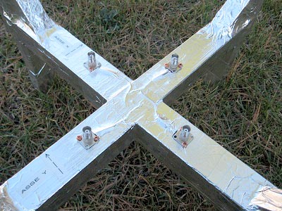 |
| FIG. 6.4 Shielding with four interruption point at the upper cross junction | FIG. 6.5 BNC sockets |
Finally, we have soldered the ends of the windings to the internal poles of two BNC female connectors for each loop
and we have connected the BNC connector bodies to the shield using copper screws. Note: if in the loop they were present iron parts (screws or angular brackets, for example), the system would work equally, but it would be less accurate in RDF applications. After the construction of the loop, we tested their electrical characteristics. Using a RCL bridge, we have measured, for various frequency, the resistive and reactive components of the loop impedance, obtaining a good compliance with the design specifications (see chapter 3).
The second part of the system encountered by the signal is the preamplifier and amplifier stage. In the chapter 5) you can find a description of the circuit operation theory. Here we want focus attention on the object manufacturing. There are several possibilities to realize the object of our interest, but it's clear that, at present, the most reasonable thing to do is to choose a solution that allows to make changes to the circuit (if necessary); after all we are in a prototyping phase. So we could choose between:
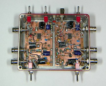
1) dead bug mounting;With the dead bug mounting it's possible to realize circuits whose behaviour reflects quite closely that of the realizations on printed circuit, especially with regard to the parasitic capacitances. On the other hand, however, it's quite difficult to make changes to the circuit during test or trial activity. With matrix board mounting we can create circuits arranged rationally and accurately, but, for example, we don't have the presence of an efficient ground plane. Also in this case, it's not easy to make changes to the circuit, when necessary.
2) matrix board mounting;
3) breadboard mounting.
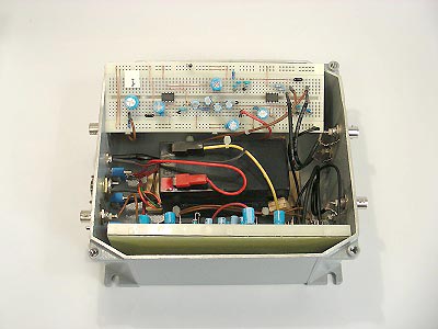
The breadboard mounting allows the realization of circuits well arranged, but we must take into account the presence of parasitic capacitance due to the mounting board. On the other hand, it's very easy to change a components in the circuit or modify the wiring. Based on these considerations, we chose to develop a prototype using the breadboard mounting, according to the scheme introduced in chapter 5). The Fig. 6.6 shows our realization. We have used two breadbord, one for each measurement axis we are interested in.
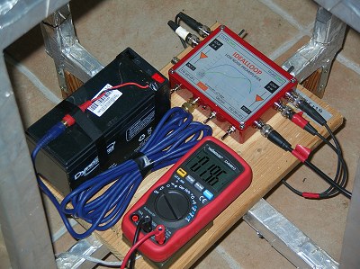
Finally we placed the two circuits mounted on breadboard inside an aluminium case with the battery providing 12 V dc power supply. On the case we put the command devices for switching on, for the choice of the response type (flat / comp)
and the BNC connectors for receiving loops. We chose an aluminium box to ensure the shielding of the circuit against the effects of electric field. The case is electrically connected with the aluminium shield tape that we have provided around the supports of the loop.
 |
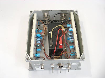 |
| FIG. 6.6 Breadboard prototype | FIG. 6.7 Case containing the preamplifier and amplifier |
6) CHARACTERIZATION
The characterization of our device has been performed in laboratory, but to do this we had to turn almost all electrical devices off, because the field they generate saturated the loop under test. We have therefore used a battery powered oscilloscope, a laptop running on batteries it also, and a function generator, supplied by network but positioned 8 meters away from the loop. Even the energy saving light bulbs had to turn off.
To perform the characterization we used a transmitter loop: it is made from 40 turns of square shape of side 45 cm.
In series with the loop is placed 1000 ohms resistance (measured 998 ohm). The resistance performs two functions: first it works as a shunt, we read with oscilloscope the voltage on it, and so we know the current flowing in the loop. By the current flowing in the loop we can calculate the generated field. The second function is to worsen the loop Q factor: in this way the current is maintained constant in all audio frequency range, from 1 Hz to 20 kHz in +/- 3 dB (connecting the function generator directly to the loop that does not happen, because of inductive reactance at high frequencies).
Transmitter loop and receiver loops (here in orthogonal version) were placed as shown in figure, 85 cm away from one another (picture left, below), and away from the function generator and as far as possible from the other laboratory instruments. The loop under test was oriented to have the lowest possible hum noise. Obviously the loop under test and the transmitter loop must be positioned on the same axis, and perfectly parallel. The table is made of wood, and there are not large ferrous metal objects nearby, that may distort the field.
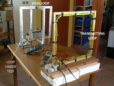 |
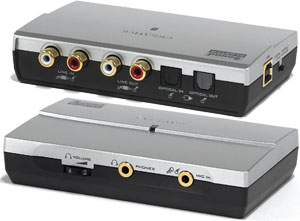 |
We have used to receive the test signal a Creative SB0270 soundcard, chosen because it performs extended linearity down to 1 Hz without any hardware modify, using LINE input. It is no longer produced by Creative but it is easy to find on ebay for a few dozen €uro. Windows mixer audio on PC was set to maximum volume and IdealLoop circuit gain set to MID value. The loop transmitter has been driven with a standard laboratory function generator, by adjusting the amplitude to obtain 100 mV voltage drop on 1000 ohm R shunt: that means 0.1 mA flowing in the loop. With this current, using Biot Savart formula (or Eric Dennison calculator http://www.netdenizen.com/emagnet/offaxis/iloopcalculator.htm) we can calculate a generated field of 241.3 pT 85 cm away, where the receiving loop is placed. Formulas are for loops of circular form, so we considered our square loop as a loop round of equal area.
At this point, we ran recordings of wave files with a sampling rate of 48000 S/s, in the following ways:
- Soundblaster SB0270, LINE input terminated on 1 kohm resistance (any signal)
- Function generator in SB0270 LINE input, 100 mVrms, 15 sec each frequency: 1, 3, 10, 30, 300, 1k, 3k, 10k, 20k Hz
- Idealloop HIGH gain, FLAT filter, with dummy loop
- Idealloop (AD797 frontend temporarily replaced with OP27) HIGH gain, FLAT filter, with dummy loop
- Idealloop HIGH gain, COMP filter, with dummy loop
- Idealloop MID gain, FLAT filter, aerial Loop, 241 pT signal test at: 1, 3, 10, 30, 300, 1k, 3k, 10k, 20k Hz
- Idealloop MID gain, COMP filter, aerial Loop, 241 pT signal test at: 1, 3, 10, 30, 300, 1k, 3k, 10k, 20k Hz
To elaborate the measures, reading the files, has been set an Hanning type window and a FFT of 65536 points. It provides a equivalent noise bandwidth of 1.00937 Hz for bin, so that we can consider the noise values read as valid: they are usually expressed in 1 Hz resolution bandwidth.
Let's see what happens for example, with gain set HIGH, aerial loop replaced with dummy loop and filter first in COMP (red curve) and then in FLAT (violet trace). Soundcard background in in green:
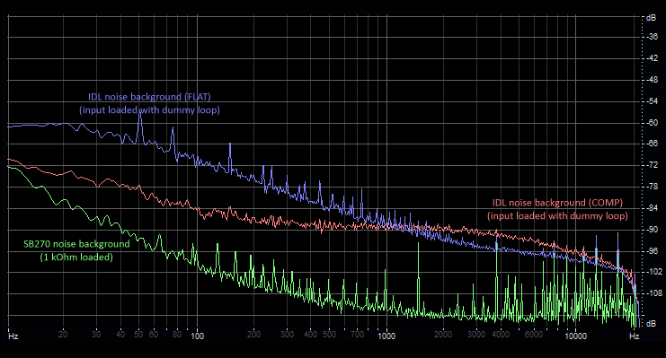
The COMP Filter reduces the distance from background noise of the sound card: this means that with gain set on MID or LOW at low frequencies the sensitivity of the system is reduced. The thing is rather guessed, but here we also measured it.
But let the numbers. Here is the table of the data acquired with audio files and graphs that show the sensitivity curve of the system in the positions of FLAT and COMP (the values indicate at each frequency the minimum detectable signal, able to exit the intrinsic noise of the system) and the frequency response of the system in the two positions:
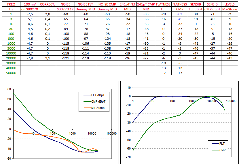
The two sensitivity curves indicate that where it is possible the FLAT position ensures maximum sensitivity, always refer to the values indicated by Maxwell and Stone in their famous paper in dBpT in 1 Hz RBW. Also the frequency responses of the system are coherent with those we had previously calculated: we have done a good job! Now we have a small and portable system, able to receive very weak signals, and with an amazingly frequency response from 8 Hz to 20 kHz in +/- 3 dB flatness.
We can obtain similar results by reasoning in another way also; in particular we can consider the signal path and the amplification of the various stages encountered. So, examining the recorded spectrograms, we can read the measured values at the various frequencies. Then, using a circuital simulation software, we can determine the receiver amplification and, considering the audio card also, the total amplification of the system.
Using these amplification values, we can determine the signal levels at the audio card and, then, at the receiver input. The level at the receiver input is equal to the voltage induced in receiving loop by the variable magnetic field. From this voltage we can obtain the relative induction value and this is the measured induction.
The tables below show the amplification encountered by signal and the diagrams indicate the effective induction value (generated during the test) and the measured value, showing, in this way, the frequency response and flatness of the system.
FLAT response case:
COMP response case:
7) POSSIBLE VARIATIONS AND TOLERANCES
Loop dimensions are not critical: it can be one centimeters larger or smaller without significantly changing the final result. Even the turns number must not necessarily be respected exactly: 5 turns more or less does not make a difference.
The presence of the screen, made of aluminium tape, helps to reject the electric field, even if it is already in part refused by the adopted configuration that performs a high CMMR. It is therefore not essential to the operation, but it improves.
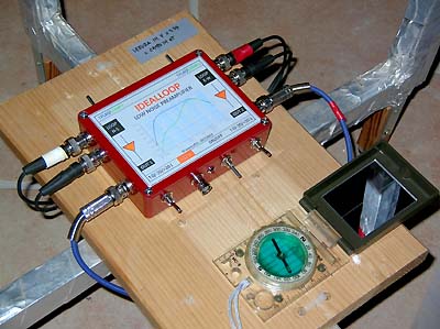
The circuit works in low frequency then it also works fine assembled on the breadboard. But for a stable and definitive solution it is appropriate to adopt an other constructive solution: here below it is an example of dead bug mounting. Beside
a circuit a compass was glued, to be able to accurately orient the loop and make the most of the function RDF.
 |
 |
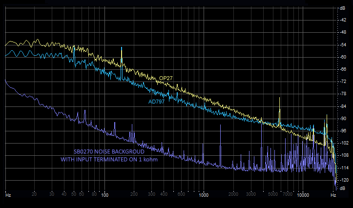
Also the choice of the input operational amplifier is not decisive hundred percent: the preamplifier also works with a different operational but can change greatly the performance in terms of input noise, and then consequently to input sensitivity. Here's an example of the dummy loop connected to the preamplifier circuit, with gain set to HIGH. Replacing the first stage, OP027 and AD797 in the two examples, the noise input changes and with it also the system sensitivity.
This means that none of the mentioned parameter is extremely critical, but the respect of all it helps to have an excellent final result.In the first draft version of the project, the loop preamplifier was calculated to give a bandwidth with a flatness within +/- 3 dB, starting from 1 Hz. The idea of having a loop totally flat from 1 Hz was intriguing. But field trials have suggested to amend specifications: the loop was perfectly flat but the intrinsic noise of the device under 10 Hz was very high. Furthermore the high sensitivity at 1 Hz made him affected by microphone effect: was enough a breath of weak wind, or someone who was walking nearby, to saturating the input, due to the Earth's magnetic field. For this reason, the input circuit has been adapted to the current form, by starting the band flatness from 8 and not from 1 Hz.
The extreme bandwidth flatness, when it is used in FLAT, allows us to use this loop also as a low frequency magnetic filed meter. This measurement can be performed by connecting the loop output to a digital multimeter or a portable oscilloscope and measuring the signal level. Once you know the level, knowing the ANTENNA FACTOR too, we can calculate the field. Let's see how to obtain the antenna factor.
We have take again the transmitter loop, made from 40 turns of square shape of side 45 cm. The ideal loop was placed 2 m away from it, with transmitting and receiving loop on the same axes (face to face) like in chapter 7, characterization. Ideal loop was set with filter FLAT and gain MID, and a portable oscilloscope was connected to its line output. A function generator was connected to the transmitting loop, a 49 ohm resistance placed in series, and a 50 Hz sine wave was injected in it (loop + resistance). Then we have increased the input signal level, until the receiving loop output, reading with the oscilloscope, was of 1.000 Vrms.
Made this we moved the oscilloscope to read the voltage across the resistor in series with the transmitter loop, and then calculate the current that flows in it. Reading was 1.477 Vrms which correspond to a 30.14 mA current. With this current, using Biot Savart formula (or again Eric Dennison calculator http://www.netdenizen.com/emagnet/offaxis/iloopcalculator.htm) we can calculate the generated field which causes an output voltage of 1.000 Vrms from the ideal loop. It is found to be of 5.966 nT. This means that @ 50 Hz: 1V = 5966 pT= 5.966 nT, or better 1mV = 5.966 pT, and then:
 |
How we can use
this value? It is simple. If in a field session we
connect a digital multimeter to the Ideal Loop
line output, set with MID gain and FLAT filter. Here beside an example in my lab: reading an AC voltage value of 0.196 V (196 mV), we are now able to calculate the field: Field [pT]= 196 mV x 5.966
pT/mV = 1169 pT
...or if you prefer 1.169 nT. The inside of my workshop is not a good place to do VLF reception, but I already knew that. Now our loop is no longer just a loop receiver, but it has also become a measuring instrument: a field strength meter. |
9) WHAT THE IDEALLOOP IS ABLE TO RECEIVE AND WHAT NOT
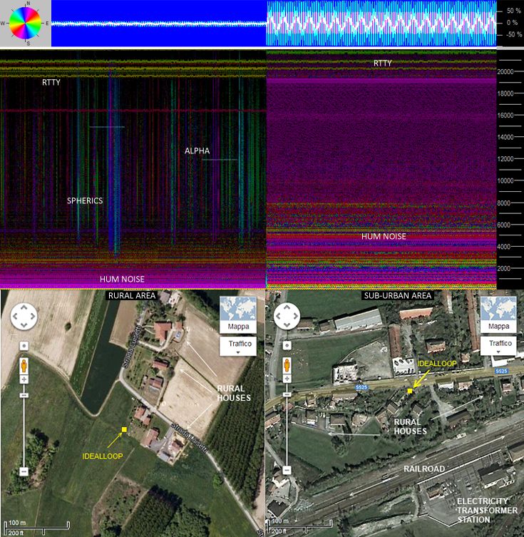
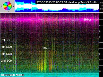
This device is able to receive, with a high degree of sensitivity, all the typical VLF radionature signals: whistlers, tweeks, chorus, hiss, statics etc. It is also able to detect the RTTY signals up to 50 kHz: for this reason it is suitable for SID monitoring. Here below panoramic reception in the VLF spectrum with "ordinary signal": RTTY, APHA, STATICS and hum noise, comparing two different receiving places.
 |
|
| Reception
taken 30 m away from home, in the middle of
the country (IdealLoop is represented by the
yellow square). |
Signal
picked up in a quasi-country place but in
sub-urban area, the IdealLoop is placed in the
middle of an house garden |
This picture teach us that one thing is an "IdealLoop", while another is to have an "ideal place": any receiver is able to receive a clean signal in the wrong place, and even the places that at first sight look good may hide disturbances.
 |
|
In the low
frequency the IdealLoop sensitivity is not enought
to detect ZEVS signals, direct to submerged
submarines, while Schumann resonances are weakly
detectable, especially from the second one (14
Hz). This device is not able to receive
geomagnetic pulsations: to receive these signals
with a loop of 50 cm side they need at least 5 kg
of copper wire, instead of 500g each loop used in
this project. The presence of filters and the gain setting allows you to use this loop virtually anywhere without saturating. It however does not mean that it is able to receive signals of radionature everywhere. |
If placed on the balcony of a city apartment it will be able to receive signals from monitors, switching power supply, energy saving lamp and any other device that is operating close to it, but probably not the signs of radionature. It does not mean that it does not work but the place is not suitable.
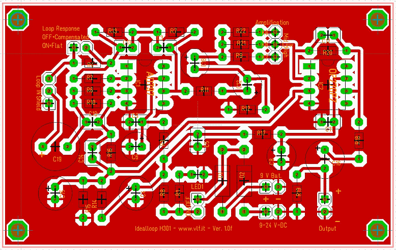
10 A) PCB Layout, by Jochen Richert
 |
| IdealLoop scheme, designed with Target 3001! PCB CAD V18 (freeware software http://www.ibfriedrich.com/ibf/en/index.html) |
Dowload source file from here:
- Target file (contain scheme and PCB): Idealloop-H301-V1f.T3001
- Eagle scheme file exported from Target: Idealloop-H301-V1f.sch
- Eagle PCB file exported from Target: Idealloop-H301-V1f.sch
With some recent versions of Eagle, in May 2020, Phil Gillaspy reports that some pads related to integrated circuits are no longer reproduced correctly, causing short circuits between the pins. Here are the correct files for recent versions of the Eagle software:
 |
 |
|
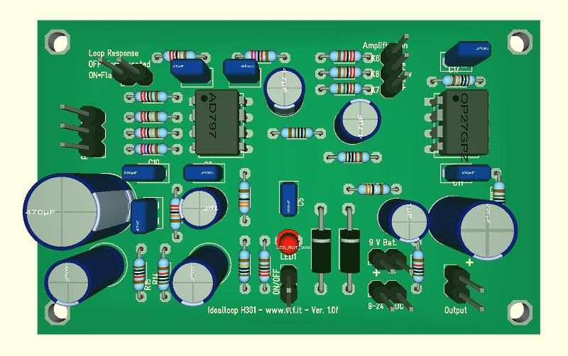
| 3D
top view realized with Target |
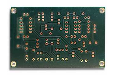
PCB
realized, bottom view |
Component List:
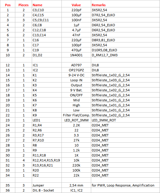
 |
| PCB top view with components and their position |
10 B) PCB Layout, by Maurizio Pallotta (Nov. 2025)
A more recent version of the PCB, created with Altium Design, is presented here, with SMD components. The connectors are positioned directly on the PCB, so no wiring is necessary. Each board also has space to house a 9V battery to power the circuit.
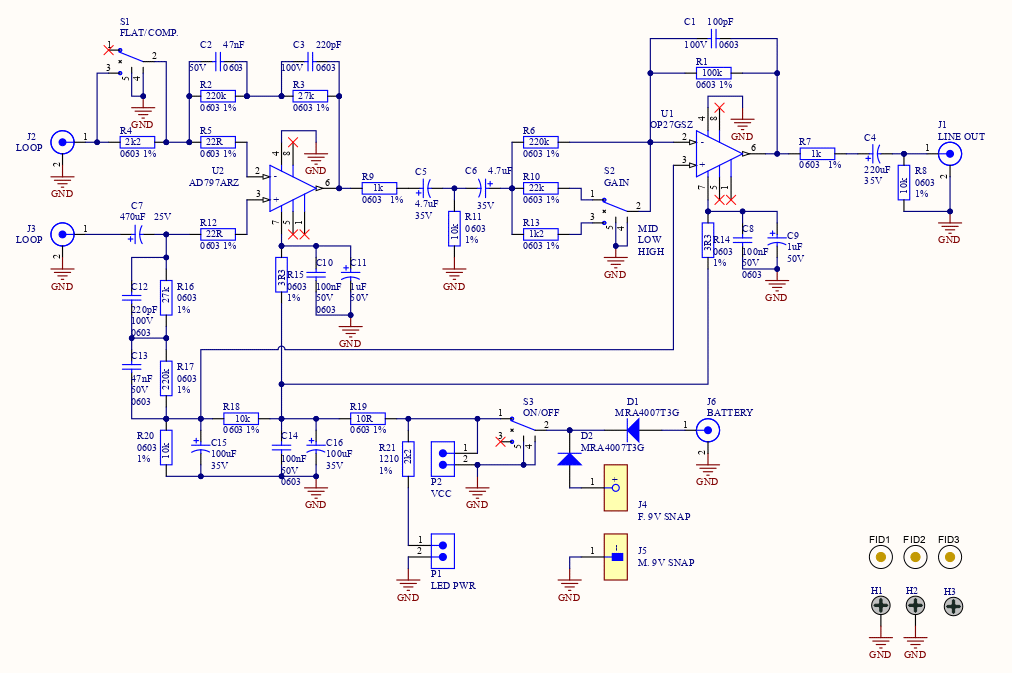
This is the starting wiring diagram.
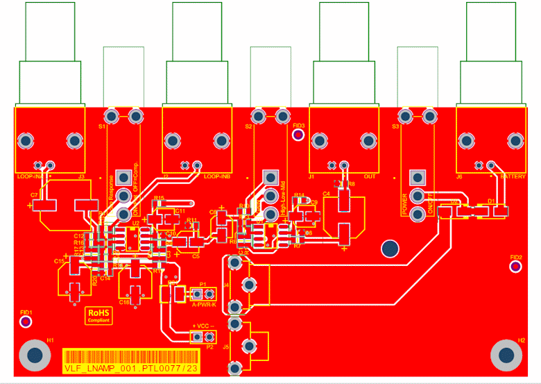
This is the PCB that was created.
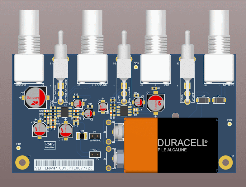
This is the simulation
 |
 |
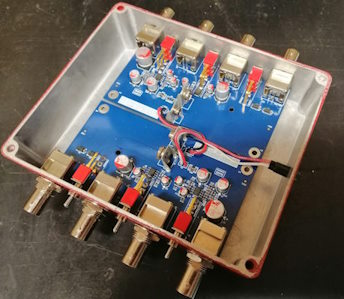
| And this is the actual circuit
assembly... |
...and the pair of orthogonal
loops. |
A PDF file containing the wiring diagram, PCB, parts list, and assembly instructions is available here:
http://www.vlf.it/feletti2/pcb/_scheme-pcb-partlist.pdf
And here are the Gerber files containing precise instructions on how to build the printed circuit board: where to place the copper tracks, holes, screen prints, and insulating layers:
http://www.vlf.it/feletti2/pcb/_GERBER-VLF_LNAMP_001.rar
And finally, here is the 3D simulation (to be opened with Adobe Reader):
http://www.vlf.it/feletti2/pcb/VLF_LNAMP_001-3D.pdf
12) CONCLUSIONS AND THANKS
It 's true that we did it, and therefore it is easy for us talk right about it, but we really think this is a device with great potential, on the border between amateur and professional. One of those antennas, that for one reason or the other,
can be used with great satisfaction on every occasion. Almost like... an IDEALLOOP!
Many thanks to:
- Jader Monari for technical review (http://www.ira.inaf.it/Home.html)
- Marco Bruno for measuring instruments (www.spinelectronics.eu)
- Andrea Bertocchi for English grammar correction (http://www.vlf.it/directcontact/directcontact.htm)